

[ad_1]
- Huawei needs UB-Mesh to unify fragmented interconnect requirements throughout huge AI clusters
- UB-Mesh design blends CLOS spine with multidimensional rack-level meshes for scalability
- Conventional interconnects develop too costly at large-scale deployments
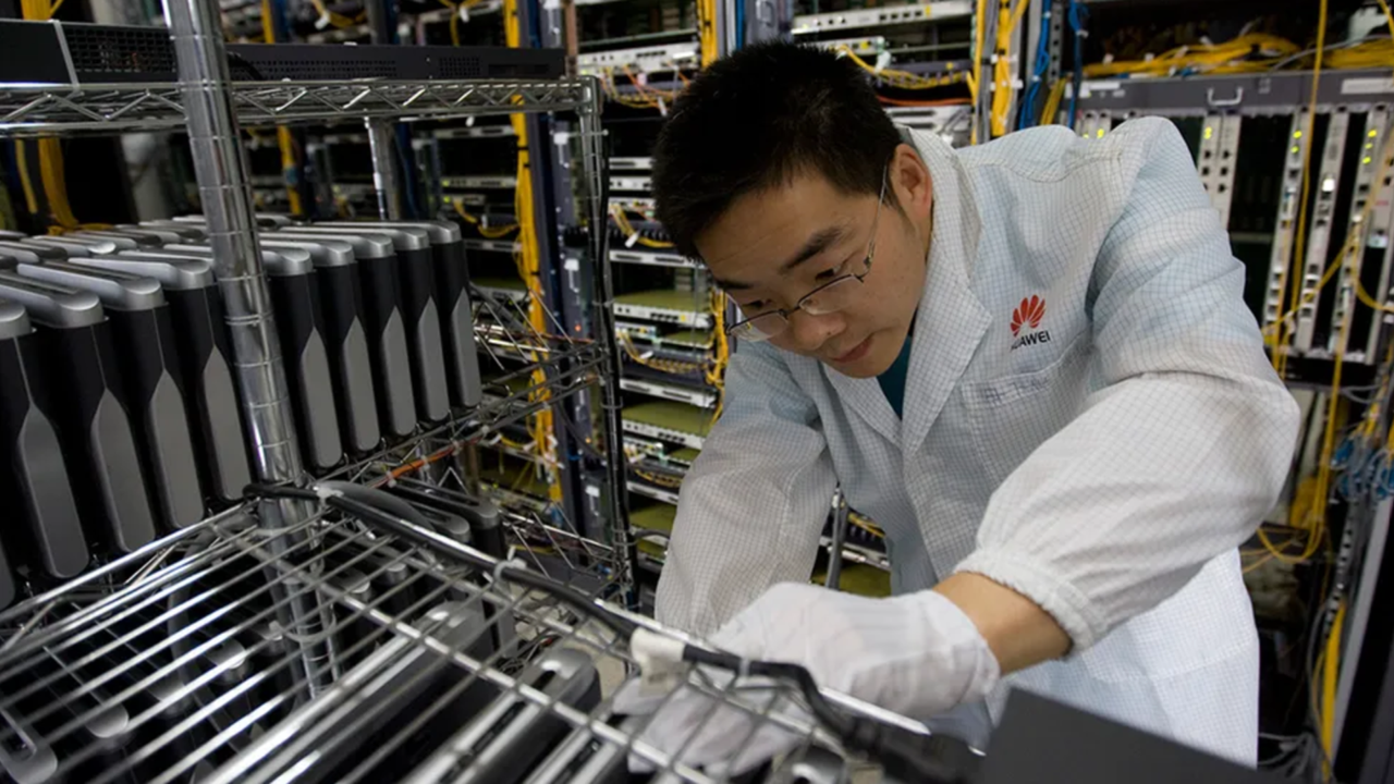
Huawei has revealed plans to open supply its UB-Mesh interconnect, a system geared toward unifying how processors, reminiscence, and networking gear talk throughout huge AI knowledge facilities.
The UB-Mesh design combines a CLOS-based spine on the knowledge corridor stage with multi-dimensional meshes inside every rack.
By combining these topologies, Huawei claims it might preserve prices beneath management whilst system sizes scale into tens of 1000’s of nodes. It additionally hopes to unravel the problem of scaling AI workloads, the place latency and {hardware} failures pose limitations.
Changing fragmented requirements with a single framework
The transfer is pitched as a option to change a number of overlapping requirements with a single framework, probably reshaping how large-scale computing infrastructure is constructed and operated.
In easy phrases, Huawei needs to switch as we speak’s combine of various connection guidelines with one common system, so all the things hyperlinks collectively extra simply and cheaply.
“Subsequent month we’ve a convention, the place we’re going to announce that the UB-Mesh protocol will likely be printed and disclosed to anyone like a free license,” mentioned Heng Liao, chief scientist of HiSilicon, Huawei’s processor arm.
“It is a very new expertise; we’re seeing competing standardization efforts from completely different camps. […] Relying on how profitable we’re in deploying precise techniques and demand from companions and prospects, we are able to discuss turning it into some form of customary.”
One of many central arguments behind UB-Mesh is that conventional interconnects develop too costly at scale, ultimately costing greater than the accelerators they’re meant to attach.
Huawei factors to its personal demonstrations, the place an 8,192-node deployment was used as proof that prices don’t must rise linearly.
That is framed as important for the way forward for AI techniques constructed with thousands and thousands of processors, high-speed networking gadgets, and large storage arrays such because the largest SSD techniques utilized in cloud storage operations.
UB-Mesh is a part of a broader thought Huawei calls the SuperNode. This refers to an information center-scale cluster the place CPUs, GPUs, reminiscence, SSD models, and switches can all function as in the event that they had been inside a single machine.
Bandwidth claims of over one terabyte per second per system and sub-microsecond latency are being positioned as proof that the idea isn’t solely potential however essential for next-generation computing.
Nonetheless, requirements like PCIe, NVLink, UALink, and Extremely Ethernet have already got backing from a number of corporations throughout the semiconductor and networking industries.
The query now’s whether or not the {industry} will settle for a brand new Huawei-backed protocol or proceed favoring requirements already supported by a wider vary of corporations.
Huawei’s proposal, whereas bold, locations prospects within the place of adopting a protocol owned and managed by one provider.
Even with open-source licensing, there are considerations about long-term interoperability, governance, and geopolitical dangers.
That mentioned, Huawei’s technical potential sounds spectacular, however its transfer calls for a level of industry-wide belief and adoption that it has but to safe.
Through Toms {Hardware}
You may also like
[ad_2]